

")
Important: The printed circuit boards are prepared for different assembly variants, components are not required in all component positions. Assembly variants are marked in the circuit diagram by connections which do not run vertically or horizontally. Familiarize yourself with the schematic diagram (SCSI2SD Mod, SCSI2SD Proc), the bill of materials and the PCB first.
Practical help for soldering SMD components is offered by all kinds of tutorials on the internet, e.g. www.mikrocontroller.net
Should individual components become unusable during assembly, they can be reordered from our webshop (observe the minimum order value!)
SCSI2SD Kit Mod (module version):
-
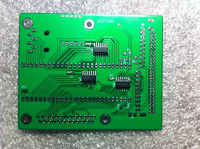
Solder components on bottom side
-
Solder SMT components on top side
-
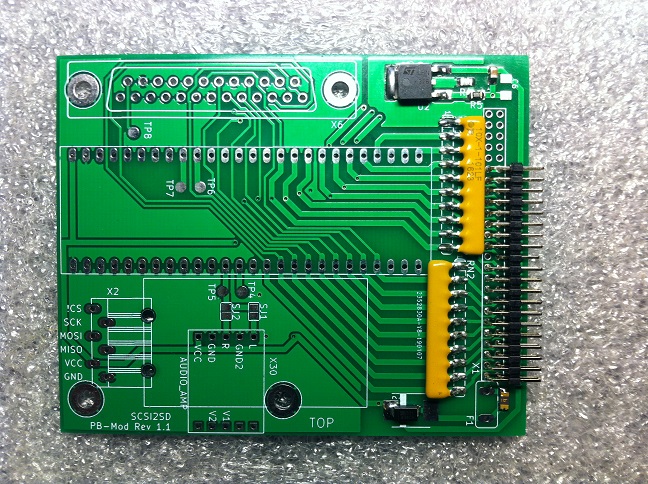
Prepare the 6-pin microSD card connector: fit into the plated through holes and solder the 6 pins.
If a flat (Arduino type) connector is used: bend 2 x 3 connections each 90°, so that zigzag pattern is created. You can solder a piece of wire across the connector to press it against the PCB. -
Solder SCSI terminating networks, make sure to pay attention to the orientation (center point = dot marking on 2.85V supply) There are three options:
a. lying down on the THT pads - yields the flattest variant, desoldering by lifting individual pins is relatively easy
b. upright in 10-pin sockets (not included) or split 20-pin IC sockets, making the assembly quite high, but networks easily removable
c. upright in THT holes. Difficult to desolder from the plated-through THT pads, not recommended.
-
Program the module CY8CKIT-059, configure it with the program SCSI2SD-util, then desolder 7 components: C41, C42 (22p 0402), C7, C9, C12, C13 (1u 0603), R5 (0R 0603), then disconnect (snap-off) programmer
This step is omitted in the Easy version, the module of this version is already programmed and modified appropriately. It is preconfigured to SCSI ID 1, the configuration can be changed at any time with SCSI2SD-util.
-
Solder the module CY8CKIT-059 onto the SCSI2SD PCB, there are 3 options:
a. Using 52 about 8mm long pieces of wire: leave about 3mm distance between the circuit boards, with around 1.6mm PCB thickness, the wire should protrude then still about 1mm on each side. The distance between the circuit boards should be chosen so that you can disconnect the module using a small side cutter by cutting the wires and possibly use the module elsewhere.
b. Using 2 x 26 pin male headers, 2.54mm pitch, 0.5mm post diameter.
1. Plastic header over CY8CKIT-059 recommended
2. Plastic header between SCSI2SD PCB and CY8CKIT-059 not recommended
c. Plug-in solution with female connector at the bottom (for example, 28-pin IC socket and 24-pin longitudinal split will give the matching 14 + 12 pins on each side)
-
Test SCSI2SD via USB using the SCSI2SD-monitor program, then solder the DB25 connector, if included or ordered in addition. If the data transfer to the SD card is not to take place via the external SCSI interface of the Powerbook (ie not from a built-in hard disk onto SCSI2SD), but instead you work with Disc Images, the DB25 connector does not need to be soldered in, thus offering a little more freedom in stacking during installation.
When operating the DB25 connector, SCSI2SD requires an external 5V supply (for example, can be connected on the THT pad of the F1B fuse). -
After successful test, solder the SCSI connector. The actual SCSI interface includes 40 (2x20) pins. The PCB is prepared for 50 (2x25) pins. The additional 10 pins (effectively 3 of them evaluated) are used in some Powerbooks to select the SCSI ID via hardware and thus enable the SCSI target mode. The Mod version does not evaluate the SCSI ID pins, so a 40-pin connector is included. To prevent improper soldering in the 50-pin layout on the circuit board, a THT hole may be filled with solder. One pin is already removed at the orientation pin of the SCSI connector.
-
The optional audio amplifier module can also be contacted later with short pieces of wire. Either the solder jumper SJ1 or SJ2 must be shorted by means of a drop of solder or short piece of wire from pad to pad. Depending on the speaker the volume should correspond approximately to the natural drive noise of the original PowerBook hard drive. If a 0805 resistor is soldered in place of the jumper, a different gain can be set according to the formula V=2*(22k/(10k+RSJ))
If a flat speaker is installed under SCSI2SD, ensure sufficient insulation from the PCB.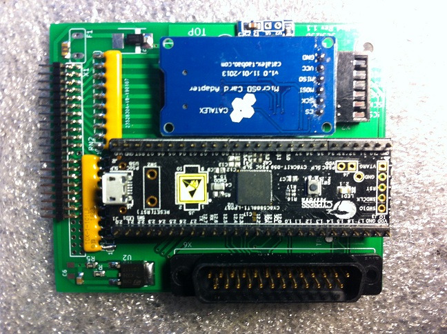
-
Think ahead how to install the assembly in place of the original hard drive by fitting the assembly under the metal cage.
a. stacked on 4 PCB holders. The PCB holders must stick to the lower shielding plate. For the two lower holders, cutouts are already cut into the gray insulating foil in the Powerbook, for the two upper ones
1. either stick the insulating film point by point to the shielding plate and glue the PCB holder onto the insulating film
2. or cut recesses into the insulating film and glue the PCB holder onto the shielding plate
b. with 4 M3 spacers (preferably made of plastic, not included) hanging from the metal cage. For this purpose, 4x 3mm holes have to be drilled in the metal cage. On the Internet there are instructional videos how holes are drilled into thin sheet metal.
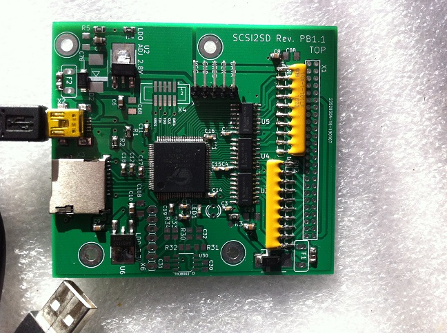
SCSI2SD Kit Proc (QFP100 processor version):
-
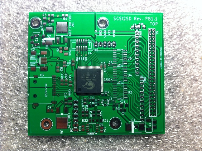
Solder U1 (PQFP100), pay attention to the orientation, compare with photos. The alignment with respect to the pads must be very accurate, it is time-consuming to de-solder a PQFP100. Visually and possibly also electrically check for contact between pin and pad, as well as unintended solder bridges between pins.
-
Solder 100nF and 1uF capacitors adjacent to U1. Without this step, programming of U1 may fail.
Steps 3-5 can be omitted if you bought a kit with a pre-programmed controller. Check the description, in doubt see the checkbox "programmed" in your bill-of-materials delivered with your kit. -
Solder 5-pin programming plug X5. First align one pin, then align pins parallel to the PCB, then solder the remaining pins. When programming with MiniProg3, solder the 10-pin SMD connector X4 (not included).
-
Connect 5-pin programming cable with programming plug X5 on one side and KitProg on the other side, pay attention to the same signals at both ends.
-
Plug KitProg into your computer's USB port and program from PSoC Programmer (or PSoC Creator), then unplug the programming cable from the programming plug.
When programming, SCSI2SD is powered from your computer via USB and then through KitProg.
-
Solder remaining SMD components, preferably the smaller ones first, then the larger ones (MicroSD, USB connectors). For diodes and ICs, it is important to observe the orientation.
-
Solder SCSI terminating networks, make sure to pay attention to the orientation (center point = dot marking on 2.85V supply) There are three options:
a. side down on the THT pads - yields the flattest variant, desoldering by lifting individual pins is relatively easy
b. upright in 10-pin sockets (not included) or split 20-pin IC sockets, making the assembly quite high, but networks easily removable
c. upright in THT holes. Difficult to desolder from the plated-through THT pads, not recommended.
-
Insert MicroSD card into socket, connect USB cable (not included) between your computer and USB connector and configure the whole module with the program SCSI2SD-util and test it with the program SCSI2SD-monitor.
During the test, the assembly is powered by USB from your computer.
SCSI2SD-monitor tests the SCSI signals with the appropriate buffers, also needs the SCSI termination networks.
SCSI2SD-monitor tests the Micro-SD interface, so it needs an inserted Micro SD card.
When configuring and testing, check the function of the LED.
-
After successful test, solder the SCSI connector. The actual SCSI interface includes 40 (2x20) pins. The PCB is prepared for 50 (2x25) pins. The additional 10 pins (effectively 3 of them evaluated) are used in some Powerbooks to select the SCSI ID via hardware and thus enable the SCSI target mode. The first software versions do not evaluate the SCSI ID pins, so a 40-pin connector is included. To prevent improper soldering in the 50-pin layout on the circuit board, a THT hole may be filled with solder. One pin is already removed at the orientation pin of the SCSI connector.
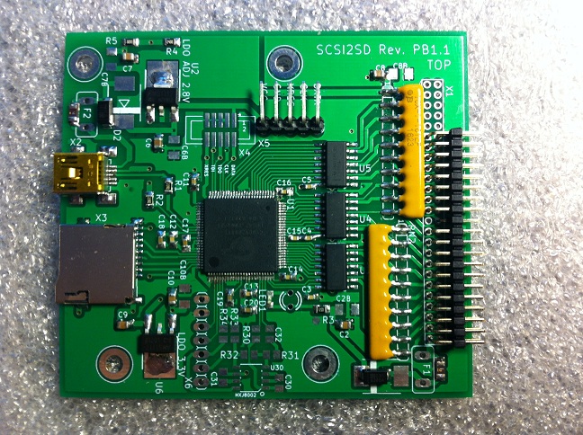
- The audio amplifier around U30 should be populated only if you intend to connect a speaker. The gain can be set according to the formula V=2*(R32/R31). Standard values are R31=R32=22k. If a flat speaker is installed under SCSI2SD, ensure sufficient insulation from the PCB. X6 is a spare GPIO header.
-
Think ahead how to install the assembly in place of the original hard drive by fitting the assembly under the metal cage.
a. stacked on 4 PCB holders. The PCB holders must stick to the lower shielding plate. For the two lower holders, cutouts are already cut into the gray insulating foil in the Powerbook, for the two upper ones
1. either stick the insulating film point by point to the shielding plate and glue the PCB holder onto the insulating film
2. or cut recesses into the insulating film and glue the PCB holder onto the shielding plate
b. with 4 M3 spacers (preferably made of plastic, not included) hanging from the metal cage. For this purpose, 4x 3mm holes have to be drilled in the metal cage. On the Internet there are instructional videos how holes are drilled into thin sheet metal.